


In the newly emerging areas in Electronics, we propose to develop VLSI Engineering Lab for students training.
Scaling of devices has been the basic principle for continuing progress in the development of VLSI. With the advancements in semiconductor manufacturing; it is becoming difficult for the VLSI designers to optimize the design without considering the effects of the VLSI processes. In the high level VLSI design, the impact of the process variation on the system performance and thus the importance of process corner analysis will be emphasized.
This subject is aimed at emphasizing the critical role of Computer Aided Design (CAD) towards VLSI design through properly embracing the high level architectural synthesis along with the low level process and device modelling. Bipolar, MOS, and BiCMOS processes will be covered. While modelling of semiconductor processing will be discussed in this subject, process and device simulation tools will be introduced in the laboratory sessions. RF and low power circuit design aspects will be covered.
The electronics industry is now the largest industrial sector in the world. The microelectronics has virtually penetrated in all consumer goods, which is a true technological revolution happened in a short span of time. The microelectronics industry needs engineers those are ready to work with little training to meet the demands of the consumers. The goal of laboratory is to produce well-trained engineers with hands-on experience to meet the rapidly changing demand of microelectronics industry. The objective of the laboratory component of any semiconductor manufacturing course is to teach the students the unit processes involved in microelectronic fabrication and to introduce the practice of process development. Computer Aided Design (CAD) for process and device simulations is now being widely used in semiconductor process design. Simulators are especially useful in microelectronics, where development cycles are long and expensive. After all it is essential for circuit and device engineers to verify the correctness of their designs before they are fabricated.
The success of a VLSI circuit design depends on the device models used to describe the device behavior. As semiconductor devices shrink, the need for accurate circuit simulation using SPICE model becomes acute. The most important component in an IC manufacturing process is the devices themselves. It is thus imperative that these devices are accurately characterized so that accurate model parameter set for the device can be extracted. The device models usually consist of a set of model equations that are either empirical or derived from device physics or a combination of both. Therefore, the design of integrated circuits is heavily dependent on circuit simulation, which needs compact device models. From the measured device characteristics, SPICE parameters are extracted. Parameter extraction is also an integral part of compact modelling. The goal of parameter extraction is to determine the values of device model parameters that minimize the total differences between a set of measured characteristics and results obtained by evaluation of the device model.
The Virtual Wafer Fabrication (VWF) has become an integral part of semiconductor fabrication. For manpower training (both via lectures and simulation laboratory), several educational institutions in the west have recently introduced courses on CAD in their curricula. With the introduction of CAD for microelectronic fabrication, it is imperative now that the teaching institutions in India introduce a new course/laboratory on Technology CAD for teaching.
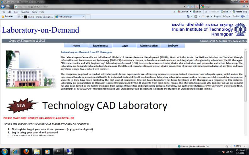
The Laboratory-on-Demand (available at http://lod.iitkgp.ernet.in/netlab/) has been an initiative to develop an online CAD laboratory. The home page for the CAD laboratory is shown in Figure 2. An online TCAD laboratory gives the student, even at the undergraduate level, a chance to learn about realistic silicon wafer processing via hands-on simulation experiments.
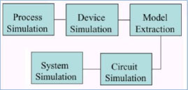
Process and device simulations are commonly used for the design of new VLSI technologies. Simulation programs serve as exploratory tools in order to gain better understanding of process and device physics. Proposed laboratory will impart “hands-on” training on all aspects of silicon and other semiconductor technology, development of new technologies and the prediction of the behavior of new device structures. The laboratory module shall have the following sessions:
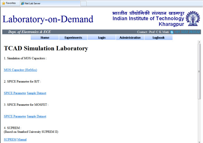
The home page for the current version of the TCAD laboratory showing various available simulation experiments is shown in Figure 5.3. In this section, we describe the outcomes for some of the above tasks:
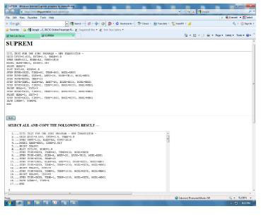
Process simulation is used during technology development to refine a process recipe, and during technology characterization to model the input structure for device simulation. Figure 4 shows the process simulation page using SUPREM.
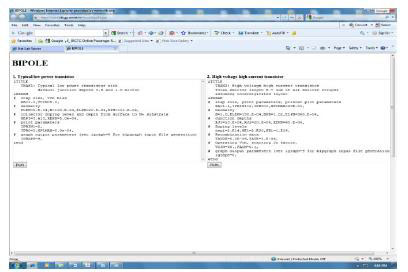
In the field of microelectronics, a device simulator is an important engineering tool with tremendous educational value. With a device simulator, a student can examine the characteristics of a microelectronic device described by a particular model. This makes it easier to develop an intuition for the general behavior of that device and examine the impact of particular device parameters on device characteristics. A device simulator lets students explore device behavior in regimes that would otherwise be infeasible or unsafe to examine. Device simulation is used to obtain simulated electrical measurements of a device, largely for technology characterization. Figure 5 shows the device simulation page for a bipolar transistor using BIPOLE device simulator.
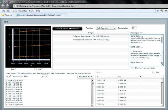
The highest level in the proposed CAD laboratory module is the SPICE parameter extraction. The main link between circuit level simulation and lower level TCAD tasks is through the compact models used in circuit simulators to characterize the behavior of individual circuit components. Simulators have tremendous educational value. With a device simulator, a student can examine how the device described by a particular model behaves when presented with various inputs. Although this exploration can be done with a real device, the appropriate equipment is often prohibitively expensive. These models are fitted to the data produced from process and device simulation, providing circuit designers with a CAD environment that accurately characterizes the manufacturing lines that will make the circuits.
Total Cost: Rs. 70.00 lakhs
 Home
Home